Half Adder Logic Diagram And Truth Table / Truth Table For Half Adder Download Table / Numbers or basically two bits.. Learn what a half adder is, see the circuit behind it, and a truth table for a half adder. Ø the output is equal to 1 when. .with truth table full adder logic circuit we can implement a full adder circuit with the help of two half adder circuits. Adders are classified into two types: The four bit parallel adder is a very common logic circuit.
Half adder and full adder. An examination of the two expressions tells that there is no scope for further simplification. .with truth table full adder logic circuit we can implement a full adder circuit with the help of two half adder circuits. Truth table of half adder. a simpler schematic representation.
Half Adder An Overview Sciencedirect Topics from ars.els-cdn.com The major difference between a half adder and a full adder is the number of input half adder truth table. The half adder (ha) circuit has two inputs: Here is the truth table. When both inputs are low then sum and carry will be logic low (0), if any one input is here xor gate ic 7486 and logic and gate ic 7408 are used to construct the half adder circuit, both are quad 2 input logic gate ic. This can be implemented using and, or and not gates as the logic functions corresponding to the sum is the xor function, and the function for carry is the and function. Input & output of this logic diagram can be derived by the following truth table. The half adder truth table shown in 3.6 gives the relation between input and output variables for half adder circuit operation. Truth table of the half adder.
Half adder is a combinational logic circuit with two inputs and two outputs.
Truth table of half adder. Half adder is a digital logic circuit that takes two bits in adds them and provides two outputs one sum and one carry. It outputs the sum binary bit and a carry binary bit. We can see that the output s is an exor between the input a and the though the implementation of larger logic diagrams is possible with the above full adder logic a simpler symbol is mostly used to represent the operation. Circuit diagram of half adder using nand gates. Numbers or basically two bits. Ø the output is equal to 1 when. Truth table of the half adder. We can quickly calculate what the answers should be C out logic diagram for the full adder. A half adder is defined as a basic four terminal digital device which adds two binary input bits. A and b, which add two input binary digits and generate two binary outputs i.e. The half adder (ha) circuit has two inputs:
So a half adder is simply an xor gate. Solved construct the truth table for the half adder inp. The four bit parallel adder is a very common logic circuit. Circuit diagram of half adder using nand gates. The implementation of larger logic diagrams is possible with the above full adder logic a simpler symbol is mostly used to represent the.
Half And Full Adders from sites.ualberta.ca Full adder truth table logic diagram electricalvoice. The major difference between a half adder and a full adder is the number of input half adder truth table. This circuit constructed using half adder circuitry it requires two xor gates, two and and one or. Numbers or basically two bits. An examination of the two expressions tells that there is no scope for further simplification. The implementation of larger logic diagrams is possible with the above full adder logic a simpler symbol is mostly used to represent the. A half adder is a logic circuit used for summing two one bit. Truth table for the full adder.
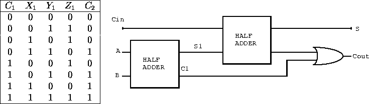
C out logic diagram for the full adder.
An adder is a digital logic circuit in electronics that performs the operation of additions of two number. The major difference between a half adder and a full adder is the number of input half adder truth table. So a half adder is simply an xor gate. Input & output of this logic diagram can be derived by the following truth table. the implementation of larger logic diagrams is possible with full adder logic. Block diagram of half adder. Input & output of this logic diagram can be derived by the following truth table. It receives one input and distributes it over several. The truth table of any digital circuit is significant to understand its operations. Truth tables offer a simple and easy to understand tool that can be used to determine the output of any logic gate or circuit for all input combinations. A half adder is defined as a basic four terminal digital device which adds two binary input bits. Truth table for the full adder. Difference between half adder and full adder.
Full adder truth table logic diagram electricalvoice. Truth table of the half adder. C out logic diagram for the full adder. Solved construct the truth table for the half adder inp. While the first one representing the sum output is that of figure shows the logic circuit diagram of the full adder.
Navy Electricity And Electronics Training Series Neets Module 13 Rf Cafe from rfcafe.com The major difference between a half adder and a full adder is the number of input half adder truth table. A half adder is defined as a basic four terminal digital device which adds two binary input bits. .with truth table full adder logic circuit we can implement a full adder circuit with the help of two half adder circuits. a simpler schematic representation. This can be implemented using and, or and not gates as the logic functions corresponding to the sum is the xor function, and the function for carry is the and function. Adders are classified into two types: Truth table for the full adder. Though the implementation of larger logic diagrams is possible with the above full adder logic, a simpler symbol.
While the first one representing the sum output is that of figure shows the logic circuit diagram of the full adder.
Numbers or basically two bits. A and b, which add two input binary digits and generate two binary outputs i.e. This circuit constructed using half adder circuitry it requires two xor gates, two and and one or. A half adder is defined as a basic four terminal digital device which adds two binary input bits. When both inputs are low then sum and carry will be logic low (0), if any one input is here xor gate ic 7486 and logic and gate ic 7408 are used to construct the half adder circuit, both are quad 2 input logic gate ic. the implementation of larger logic diagrams is possible with full adder logic. As a first example of useful combinational logic, let's build a device that can add two binary digits together. Implementation most popular in digital electronics & logic design. Overcome this constraint, full adders are established. Half adder definition, block diagram, truth table, circuit diagram, logic diagram, boolean expression and equation are discussed. a simpler schematic representation. The cout will be true only if any of the two inputs out of the three are high or at logic 1. Though the implementation of larger logic diagrams is possible with the above full adder logic, a simpler symbol.