Home
› Logic Diagram And Truth Table Of Jk : Logic Diagram And Truth Table Of Jk Flip Flop - Wiring Diagram Schemas - Block diagram, truth table, & logic diagram.
Logic Diagram And Truth Table Of Jk : Logic Diagram And Truth Table Of Jk Flip Flop - Wiring Diagram Schemas - Block diagram, truth table, & logic diagram.
Logic Diagram And Truth Table Of Jk : Logic Diagram And Truth Table Of Jk Flip Flop - Wiring Diagram Schemas - Block diagram, truth table, & logic diagram.. The t latch forms by shorting the jk latch inputs. The circuit diagram and timing diagram are given below. Sr flip flop is the simplest type of flip flops. When j = 0, k = 1, s input is at 0 while r can be either at 0 or 1, but output is always in the reset state. Truth table shows the corresponding outputs for every combination of inputs.
A bistable circuit can exist in either of two stable states indefinitely and can be made to change its state by means of some external signal. Truth table and applications of sr, jk, d, t, master slave flip flops. Here j = s and k = r. We will discuss each herein and demonstrate ways to convert between them. The jk flip flops work as storage devices, control circuits, and counters.
Sequential And Combinational Logic Circuits - The Engineering Street from 1.bp.blogspot.com Jk flip flop construction, logic circuit diagram, logic symbol, truth table, characteristic equation & excitation table are discussed. The truth tables of logic gates are very complex but larger than the not gate. There are only two changes. A, b and cin, which add three input binary digits and generate two binary outputs i.e. The truth table of each gate must include many rows like there are possibilities for exclusive combinations for inputs. Explain the working of clocked jk flip flop with its logic diagram truth table and timing asked mar 16, 2020 in electronics by richa01 ( 53.5k points) digital electronics Logic circuits are designed to perform a particular function, understanding the nature of that function requires a logic circuit truth table. With a logic circuit, explain working of unlocked sr flip flop built using nand gates.
Truth table for logic gates with 3 inputs uncategorized september 19, 2018 two birds home 0 3 input and gate truth table worked out digital electronics logic gates basics or multi operators its operation nand area design from function to.
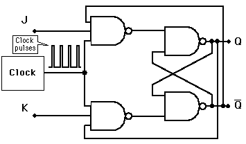
The full adder (fa) circuit has three. Explain the working of clocked jk flip flop with its logic diagram ,truth table and timing answer: These flip flops have complicated wiring and can only be used when the clock is set at high to get it activated. The jk flip flops work as storage devices, control circuits, and counters. J, k and qp make eight possible combinations, as shown in the conversion table below. We will discuss each herein and demonstrate ways to convert between them. D is expressed in terms of j, k and qp. Jk flip flop and the master slave jk flip flop tutorial The circuit diagram of the jk flip flop is shown in the figure below:. The output of the t latch toggle when the input set to 1 or high. Logic diagram and truth table of jk : Flip flop is a circuit or device which can store which can store a single bit of binary data in the form of zero (0) or (1) or we can say low or high. Here j = s and k = r.
Explain the working of clocked jk flip flop with its logic diagram truth table and timing asked mar 16, 2020 in electronics by richa01 ( 53.5k points) digital electronics It is used to find out if a propositional expression is. The full adder (fa) circuit has three inputs: The output of the t latch toggle when the input set to 1 or high. J, k and qp make eight possible combinations, as shown in the conversion table below.
J-K Flip-Flop from 1.bp.blogspot.com Asked mar 16, 2020 in electronics by richa01 ( 53.4k points) Logic diagram and truth table of jk : Jk flip flop and the master slave jk flip flop tutorial Draw its timing diagram and truth table. Analysing the above assembly as a two stage structure considering previous state (q') to be 0 when j = 1, k = 0 and clock = high Below is the circuit diagram of the t latch. A, b and cin, which add three input binary digits and generate two binary outputs i.e. Jk flip flop is a refined and improved version of the sr flip flop.
The full adder (fa) circuit has three inputs:
I) convert sr to jk flipflop A bistable circuit can exist in either of two stable states indefinitely and can be made to change its state by means of some external signal. In fact, it is a special form of the truth table that is folded upon itself like a sphere. Flip flop is a circuit or device which can store which can store a single bit of binary data in the form of zero (0) or (1) or we can say low or high. Jk flip flop logic diagram. The jk flip flops work as storage devices, control circuits, and counters. Block diagram, truth table, & logic diagram. Sr flip flop construction, logic circuit diagram, logic symbol, truth table, characteristic equation & excitation table are discussed. Adders are classified into two types: The truth tables of logic gates are very complex but larger than the not gate. Half adder and full adder. Jk flip flop construction, logic circuit diagram, logic symbol, truth table, characteristic equation & excitation table are discussed. Here j = s and k = r.
The circuit diagram and truth table of the jk latch are as follows: The truth tables of logic gates are very complex but larger than the not gate. This is known as a timing diagram for a jk flip flop. When j = 0, k= 0, the s and r inputs are both at 0 and hence the output is in the hold state. These flip flops have complicated wiring and can only be used when the clock is set at high to get it activated.
Digital Logic - learn.sparkfun.com from dlnmh9ip6v2uc.cloudfront.net The circuit diagram and truth table of the jk latch are as follows: Truth table for logic gates with 3 inputs uncategorized september 19, 2018 two birds home 0 3 input and gate truth table worked out digital electronics logic gates basics or multi operators its operation nand area design from function to. Analysing the above assembly as a two stage structure considering previous state (q') to be 0 when j = 1, k = 0 and clock = high Sr flip flop construction, logic circuit diagram, logic symbol, truth table, characteristic equation & excitation table are discussed. Logic circuits are designed to perform a particular function, understanding the nature of that function requires a logic circuit truth table. The s and r inputs of the rs bistable have been replaced by the two inputs called the j and k input respectively. The truth tables of logic gates are very complex but larger than the not gate. Jk flip flop logic diagram.
Truth table for logic gates with 3 inputs uncategorized september 19, 2018 two birds home 0 3 input and gate truth table worked out digital electronics logic gates basics or multi operators its operation nand area design from function to.
In fact, it is a special form of the truth table that is folded upon itself like a sphere. Logic circuits are designed to perform a particular function, understanding the nature of that function requires a logic circuit truth table. Flip flop is a circuit or device which can store which can store a single bit of binary data in the form of zero (0) or (1) or we can say low or high. This is known as a timing diagram for a jk flip flop. The jk flip flop was termed after his inventor jack kilby which is available as ic packages. Explain the working of clocked jk flip flop with its logic diagram truth table and timing asked mar 16, 2020 in electronics by richa01 ( 53.5k points) digital electronics Construct logic diagram according to the functions obtained. An adder is a digital logic circuit in electronics that performs the operation of additions of two number. As here 'n' value is three, the counter can count up to 2 3 = 8 values.i.e. Logic diagram and truth table of jk : Before we learn what a jk flip flop is, it would be wise to learn what, actually, a flip flop is. Sr flip flop construction, logic circuit diagram, logic symbol, truth table, characteristic equation & excitation table are discussed. Jk flip flop construction, logic circuit diagram, logic symbol, truth table, characteristic equation & excitation table are discussed.